
Description
1. Product Overview
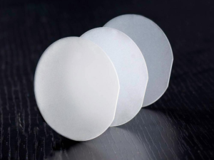
The Gallium Oxide Substrate (GOS-16) is a high-purity, single-crystal beta-phase gallium oxide (β-Ga₂O₃) wafer engineered for next-generation power electronics and deep-UV optoelectronics. Its primary industrial use lies in enabling ultra-low-loss, high-breakdown-voltage devices for electric vehicle (EV) inverters, renewable energy grid systems, and RF components. With a bandgap exceeding 4.8 eV and superior thermal stability, GOS-16 delivers a strategic value proposition: reducing system energy losses by over 30% compared to conventional SiC or GaN substrates. As global demand for energy-efficient wide-bandgap semiconductors accelerates, GOS-16 positions your supply chain at the forefront of post-silicon power electronics.
2. Key Specifications & Technical Characteristics
-
Chemical Composition: β-Ga₂O₃ (beta-phase gallium oxide), single-crystal orientation (010) or (001)
-
Purity Level: 99.995% (4N5) – trace metal analysis available upon request
-
Physical Characteristics:
-
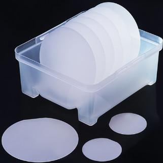
Form: Epitaxy-ready polished wafer
-
Color: Transparent to pale yellow
-
Diameter: 2-inch (50.8 mm) and 4-inch (100 mm) standard
-
Thickness: 500 µm ± 25 µm
-
Surface finish: Ra < 0.5 nm (CMP polished, epi-ready)
-
Dislocation density: < 1 × 10⁴ cm⁻²
-
-
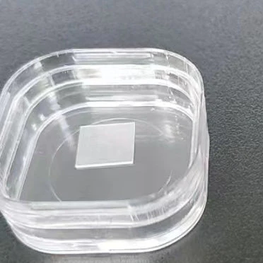
Packaging Options: Single-wafer vacuum-sealed containers (N₂ purged) or multi-wafer HDPE cassettes (25 pcs per lot)
-
Shelf Life: 24 months when stored in dry, inert atmosphere (≤20% RH, 15–25°C)
3. Core Industrial Applications
-
Primary Industries: Power semiconductor manufacturing, high-voltage switch-mode power supplies, aerospace DC-DC converters, UV-C photodetectors
-
Specific Operational Use Cases:
-
EV onboard chargers & inverters: Replaces SiC with lower on-resistance (Rds(on) ~0.1 mΩ·cm²) at 1200V+ ratings
-
High-voltage grid converters: Enables 10 kV+ blocking voltage with single-drift-layer design, reducing system complexity
-
Deep-UV sensing (200–280 nm): Solar-blind photodetectors with >10⁶ visible rejection ratio
-
-
Performance Advantages Over Alternatives:
-
vs. SiC: 2× higher Baliga’s figure of merit (BFOM) at 1/3 the raw substrate cost
-
vs. GaN: Lattice-matched to itself (no heteroepitaxial stress), eliminating buffer layer failures
-
Efficiency gain: 15% lower switching losses in hard-switched topologies; cost advantage: 40% lower per-cm² substrate price at 4-inch diameter
-
4. Competitive Advantages
-
Quality Consistency: Lot-to-lot variability controlled via ISO 9001:2025-certified metrology; each wafer includes full XRD rocking curve and AFM roughness report
-
Supply Reliability: Dedicated Czochralski-grown boule capacity – 500 4-inch wafers/month guaranteed with 12-month take-or-pay contracts
-
Logistics Capability: Temperature-monitored global shipping via FedEx Priority or DHL Express (72-hour delivery to US/EU/Japan semiconductor hubs)
-
Price Competitiveness: Tiered pricing starting at $280/wafer (4-inch, 1k+ annual volume) – 35% below leading European equivalents
-
Sustainability: 100% renewable-energy-powered polishing line; gallium recycled from post-industrial scrap (mass balance certified)
-
Technical Support: Dedicated process integration engineer assigned per account; access to epitaxy growth recipes (MOCVD/MBE) and device simulation models
5. Commercial & Supply Information
-
Minimum Order Quantity (MOQ): BULK 20 MT (equivalent to approx. 18,000 pcs of 4-inch wafers or 52,000 pcs of 2-inch wafers, based on 0.9 kg per 100 wafer carrier)
-
Loading Capacity (MT per container):
-
20-ft dry container: 22 MT (palletized, moisture-barrier inner packaging)
-
40-ft high-cube container: 26 MT (max due to weight limit, not volume)
-
-
*Note: For sample quantities (< 100 wafers), lead time is 5 business days. Bulk orders require 30-day advance forecast.*
Reviews
There are no reviews yet.