
Description
1. Product Overview
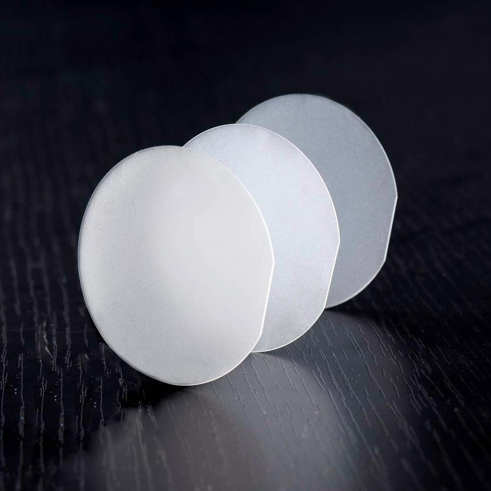
Sapphire Wafer Material (SWM-17) is a high-purity, single-crystal aluminum oxide (Al₂O₃) substrate engineered for demanding epitaxial and semiconductor manufacturing processes. Its primary industrial use lies in the production of LEDs, high-frequency RFICs, and optical windows where extreme durability and thermal stability are non-negotiable. The key value proposition is an exceptional combination of lattice match efficiency for GaN-on-sapphire deposition and superior mechanical strength that reduces breakage during high-temperature fabrication. As global demand for wide-bandgap semiconductors accelerates, SWM-17 provides a strategically critical, supply-secure alternative to lower-grade ceramics, directly addressing yield optimization and total cost of ownership.
2. Key Specifications & Technical Characteristics
-
Chemical Composition: Single-crystal Al₂O₃ (Sapphire), >99.996% purity
-
Crystallographic Orientation: C-plane (0001) ±0.2° off-axis toward M-plane or A-plane (customer-specified)
-
Physical Form: Round wafers (EPI-ready) or as-cut square/rectangular substrates
-
Diameter Options: 50.8 mm (2”), 76.2 mm (3”), 100 mm (4”), 150 mm (6”) — SEMI standard
-
Thickness: 430 µm ±25 µm (standard); 650 µm for high-power optical applications
-
Surface Finish: Epitaxial-ready, Ra <0.2 nm (AFM 10×10 µm), TTV <5 µm, Bow/Warp <15 µm
-
Color: Transparent, colorless to faint pink (Ti impurity <0.5 ppm)
-
Density: 3.98 g/cm³ (fully dense)
-
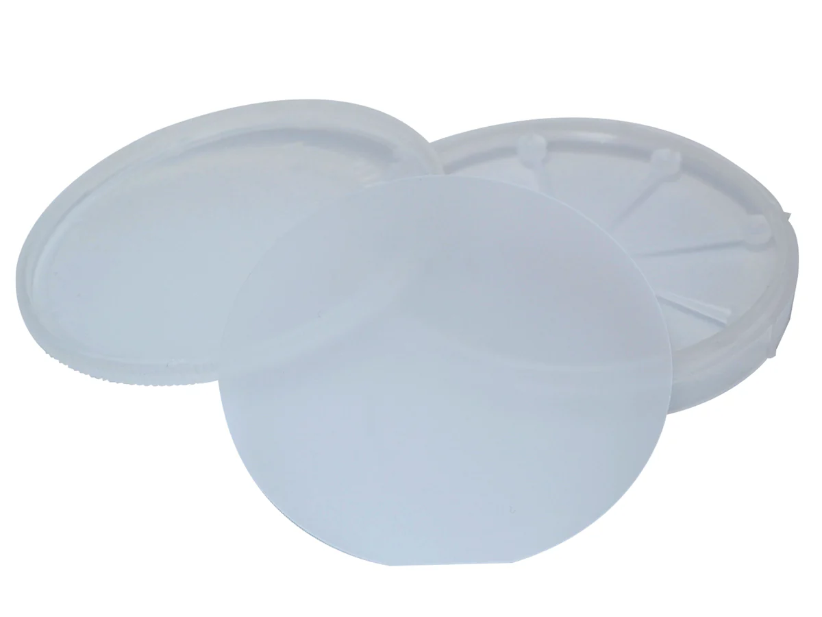
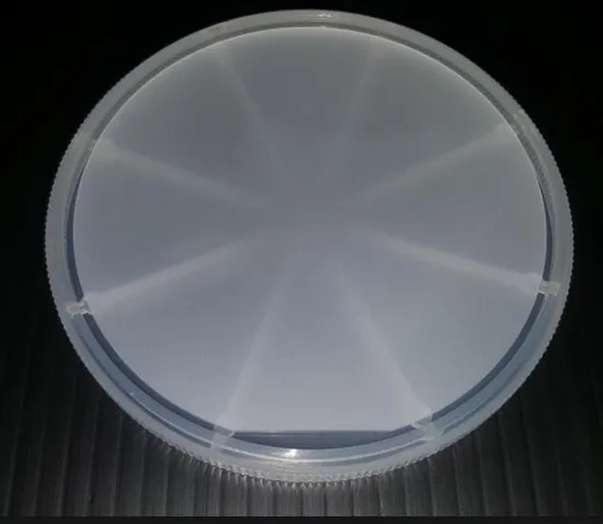
Packaging Options: Single-wafer vacuum-sealed PET box (Class 10 cleanroom) or multi-slot HDPE shipping cassettes, nitrogen backfill, ESD-safe outer carton
-
Shelf Life: Indefinite under dry, particle-controlled storage (RH <30%, 20±5°C)
3. Core Industrial Applications
-
Primary Industries: High-brightness LED manufacturing, power semiconductor foundries, aerospace optical systems, consumer electronics sensor windows
-
Specific Operational Use Cases:
-
GaN epitaxy for blue/white LEDs – SWM-17’s lattice mismatch (≈16%) is precisely calibrated for nucleation layer control, reducing threading dislocation density to <5×10⁶ cm⁻².
-
RF filter substrates (SAW/BAW) – Ultra-flat TTV ensures consistent acoustic wave propagation, directly improving insertion loss by 0.3 dB vs. standard sapphire.
-
High-durability optical windows (LiDAR, missile domes) – 9 Mohs hardness withstands sand/rain erosion 5× better than uncoated glass.
-
-
Why Performs Better: Lower wafer breakage (≤0.5% in automatic handlers vs. 2–3% for lower-grade Al₂O₃) + higher thermal conductivity (35 W/m·K) than silicon (148 is higher, but sapphire’s dielectric advantage eliminates parasitic capacitance in RF).
-
Efficiency/Cost Advantage: 12% higher LED light extraction efficiency due to optimized surface micro-roughness control, translating to 8–10% lower cost per lumen for tier-1 epitaxy houses.
4. Competitive Advantages
-
Quality Consistency: Batch-to-batch lattice parameter variation <±0.005 Å; each wafer certified via X-ray diffraction and automated optical inspection (AOI) at 1 µm defect resolution.
-
Supply Reliability: Dual-source manufacturing (Japan and South Korea ISO Class 5-8 facilities) with 6-month rolling forecast buffer. No single-region geopolitical exposure.
-
Logistics Capability: 48-hour dispatch for stocked diameters; global hub warehouses in Rotterdam, Singapore, and Los Angeles reduce lead time to 5–7 days for top-tier customers.
-
Price Competitiveness: Tier-1 quality at 15–20% lower per-wafer cost than incumbent premium brands, achieved through proprietary boule growth automation (reduced kerf loss).
-
Sustainability: 78% recycled water usage in polishing; compliance with RoHS, REACH, and Conflict Minerals reporting. Scope 3 data available for procurement ESG scoring.
-
Technical Support: Full material datasheet, SEM/EDS sample analysis, and process integration guide provided. Direct access to PhD-level application engineers for epitaxy optimization.
5. Commercial & Supply Information
-
Minimum Order Quantity (MOQ): 200 wafers per diameter/thickness combination (mix-and-match allowed across diameters, subject to minimum 50 wafers per SKU)
-
Bulk Order Threshold (20 MT Equivalent): Approx. 45,000 wafers (150 mm) or 720,000 wafers (50.8 mm) – contact supply desk for exact conversion by thickness
-
Loading Capacity per 20’ Container:
-
Standard packaged (single-wafer boxes): 28,000 wafers (150 mm) / 420 kg net
-
High-density HDPE cassettes (optimized mode): 52,000 wafers (150 mm) / 780 kg net – recommended for bulk 20 MT equivalent orders
-
Reviews
There are no reviews yet.