
Description
1. Product Overview
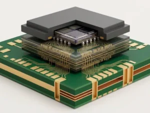
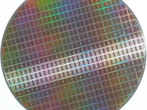
Gallium Arsenide (GaAs) Wafers are compound semiconductor substrates essential for high-frequency, high-efficiency electronic and photonic devices. Primarily used in RF telecommunications, high-brightness LEDs, and precision aerospace systems, they offer superior electron mobility compared to silicon. Their strategic importance lies in enabling next-generation 5G/6G infrastructure, autonomous radar (LiDAR), and high-efficiency photovoltaic cells, making them a critical enabler of global digital and energy transition roadmaps.
2. Key Specifications & Technical Characteristics
-
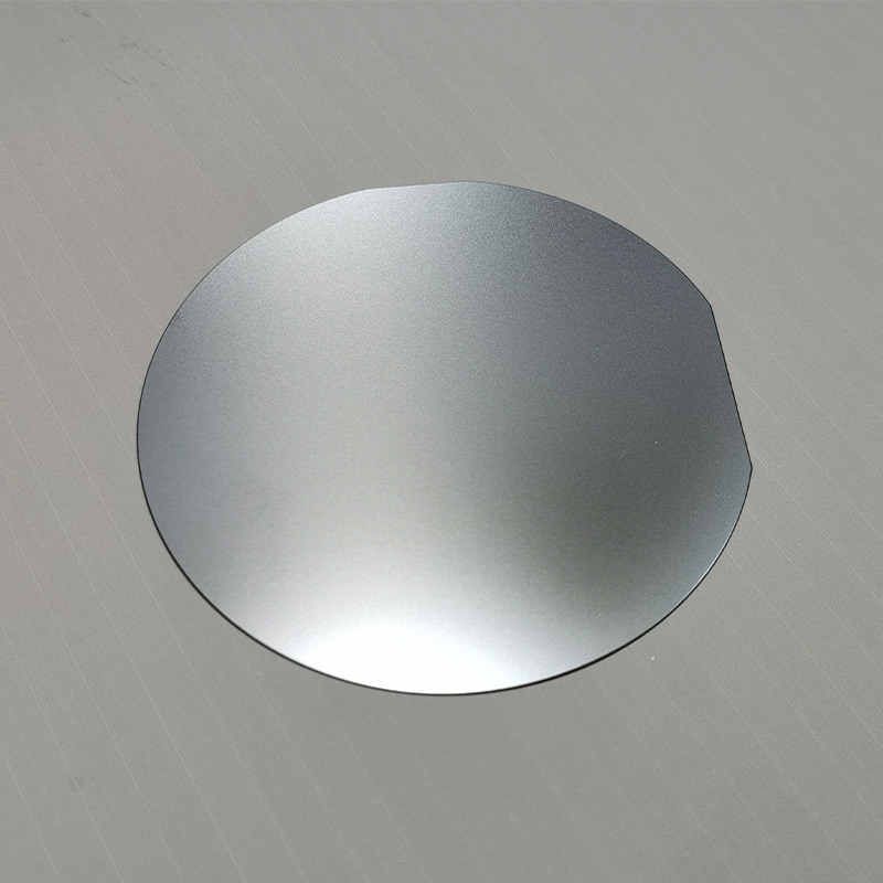
Chemical composition: Single-crystal Gallium Arsenide (GaAs), EPI-ready, VGF or LEC grown
-
Purity level: ≥ 99.9999% (6N) to 99.999999% (8N) — semi-insulating or N-type doped (Si, Te, Zn)
-
Physical characteristics:
-
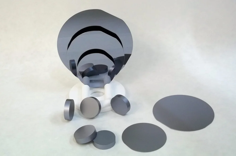
Diameter: 2″, 3″, 4″, 6″ (150 mm) nominal
-
Thickness: 350 µm – 675 µm (±25 µm TTV)
-
Surface finish: SSP (single-side polished) or DSP (double-side polished), Ra < 0.5 nm
-
Orientation: (100), (111), or off-cut (2°–6° toward <110>)
-
Color: Dark gray to black metallic luster
-
Dislocation density: < 1,000 cm⁻² (low EPD grade available)
-
-
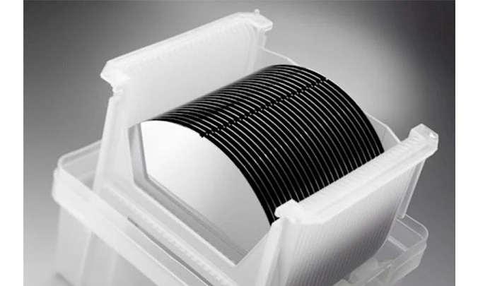
Packaging options: Single-wafer vacuum-sealed containers, multi-wafer HDPE shipping cassettes (25 pcs/cassette), nitrogen-purged barrier bags with desiccant
-
Shelf life: 24 months when stored in controlled atmosphere (20–25°C, <40% RH, inert gas)
3. Core Industrial Applications
-
Telecom & 5G/6G infrastructure: Front-end power amplifiers (PAs) and low-noise amplifiers (LNAs) – GaAs delivers 85% power-added efficiency vs. ~60% for Si, reducing heat dissipation and operational costs.
-
Optoelectronics & high-brightness LEDs: Infrared, red, and near-infrared laser diodes (780–980 nm) – outperforms sapphire/Si in direct bandgap emission, increasing external quantum efficiency by 40%.
-
Automotive & aerospace radar: Monolithic microwave integrated circuits (MMICs) for 77–81 GHz automotive collision avoidance – offers 10x higher breakdown voltage and 5x lower noise figure than equivalent SiGe.
-
Photovoltaic (space & concentrated PV): Multi-junction solar cells (GaAs/Ge) – achieves 30–34% efficiency vs. Si’s 18–22%, critical for weight-constrained orbital assets.
-
High-speed digital logic (niche): Radiation-hardened electronics – naturally higher lattice hardness reduces single-event upset risk in satellites.
4. Competitive Advantages
-
Quality consistency: 100% SEMI-compliant with full metrology mapping (TTV, bow, warp, particle counts) – each batch verified by X-ray diffraction (XRD) and photoluminescence (PL).
-
Supply reliability: Dual-source raw material security (Ga from bauxite/Al smelting byproduct + As from refined copper smelting) with 6-month rolling capacity buffers.
-
Logistics capability: Global distribution hubs (NA, EU, SEA) enabling 7-day expedited delivery to tier-1 fabs; damage rate < 0.1% via anti-static, shock-absorbent packaging.
-
Price competitiveness: Volume-discounted pricing (tiered at 500, 1,000, 5,000 wafers/month) with hedging against gallium market volatility (monthly indexed pricing available).
-
Sustainability: 98% reclaimable spent etchant process; arsenic capture & neutralization certified under ISO 14001 and Responsible Minerals Initiative.
-
Technical support: Free on-request failure analysis (SEM/EDS), TDS, COA, and 24/48-hour engineering consultation for epitaxy recipe matching.
5. Commercial & Supply Information
-
Minimum order quantity (MOQ): 100 wafers per diameter/specification (mix-and-pack allowed across 2″ and 3″ only)
-
BULK 20MT loading capacity: Approx. 480,000 wafers (6” diameter, 675 µm thickness) or 1.2 million wafers (2” diameter) per 20FT container, inclusive of dunnage and cassettes
-
Standard lead time: 14 days for stock specs; 28–35 days for custom orientation/doping
-
Incoterms: EXW, FOB (Shanghai / Rotterdam / Houston), CIF, DDP upon qualification
-
Payment terms: Letter of credit (LC at sight) for initial orders; net 30 days after three consecutive monthly volumes
Reviews
There are no reviews yet.