
Description
Product Overview
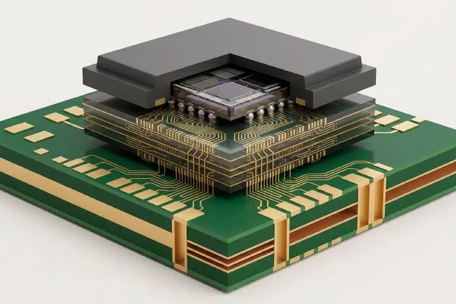
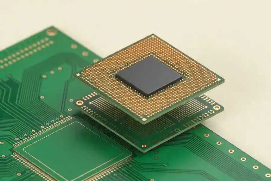
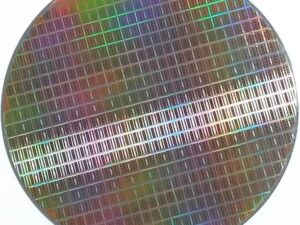
Integrated Circuit Substrates are precision-layered carrier materials that electrically connect and physically support semiconductor dies within advanced packages. Used primarily in flip-chip BGA, wafer-level packaging, and system-in-package assemblies, they deliver low signal loss and high heat dissipation. Their strategic value lies in enabling heterogeneous integration and miniaturization for next-gen electronics. As chip complexity increases, substrate quality directly determines device yield and reliability.
Key Specifications & Technical Characteristics
-
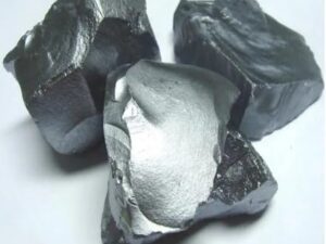
Material composition: Build-up film (ABF-like), high-Tg FR-4, or ceramic-filled resin with Cu metallization
-
Purity/grade: UL 94 V-0 flame retardant; ionic contamination < 0.05 µg/cm²
-
Physical characteristics: Rigid or thin-core (0.1–1.5 mm); panel sizes up to 600×600 mm; line/space down to 8/8 µm
-
Packaging options: Vacuum-sealed, moisture-barrier bags; JEDEC trays or vacuum-packed reels
-
Shelf life: 6 months at <30°C / <60% RH (unopened)
Core Industrial Applications
-
Primary industries: Semiconductor packaging (OSATs, IDMs), automotive electronics, high-performance computing, 5G infrastructure
-
Specific use cases: CPU/GPU substrates for servers, ADAS radar modules, mmWave antenna-in-package, power management ICs
-
Performance advantage: Lower insertion loss (≤0.1 dB/mm at 28 GHz) and 30% higher thermal conductivity vs. standard laminates
-
Efficiency gain: Reduces rework rates by enabling finer pitch (<40 µm) and warpage control ≤50 µm after reflow
Competitive Advantages
-
Quality consistency: Cpk ≥1.33 across all critical dimensions; 100% AOI + flying probe testing
-
Supply reliability: Dual-source raw materials; 12-week lead time with buffer stock in three regions
-
Logistics capability: Door-to-door with ESD-safe logistics; real-time tracking API for B2B platforms
-
Price competitiveness: Tier-1 performance at 15–20% below incumbent Japanese/Korean suppliers for equivalent layer counts
-
Sustainability: RoHS/REACH compliant; halogen-free options; recycled copper content ≥30%
Commercial & Supply Information
-
Minimum order quantity (MOQ): BULK 20MT
-
Loading capacity: 18 MT per standard 20-ft container (palletized)
Reviews
There are no reviews yet.