
Description
1. Product Overview
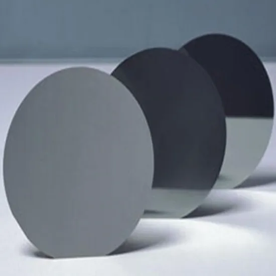
The 300mm Prime Wafer is the industry-standard monocrystalline silicon substrate engineered for advanced semiconductor fabrication at nodes ≤7nm. It serves as the foundational layer for logic, memory, and system-on-chip (SoC) devices in high-volume fabs. Its strategic value lies in maximizing die yield per wafer (2.25x area of 200mm wafers) while enabling the tightest defect density tolerances required for AI, HPC, and 5G supply chains.
2. Key Specifications & Technical Characteristics
-
Chemical composition: Monocrystalline Silicon (Si), Czochralski (CZ) or Float Zone (FZ) grown, Boron or Phosphorus doped (p-type / n-type)
-
Purity level: ≥99.9999999% (9N+), Metals content <1E10 atoms/cm²
-
Physical characteristics:
-
Diameter: 300mm ±0.2mm
-
Thickness: 775µm ±25µm
-
Warpage: ≤30µm
-
Bow: ≤20µm
-
Total Thickness Variation (TTV): ≤0.5µm
-
Surface roughness (Ra): ≤0.15nm
-
Crystal orientation: <100> ±0.5° (primary flat: SEMI standard)
-
-
Particle count: ≤15 particles (>0.12µm) per wafer
-
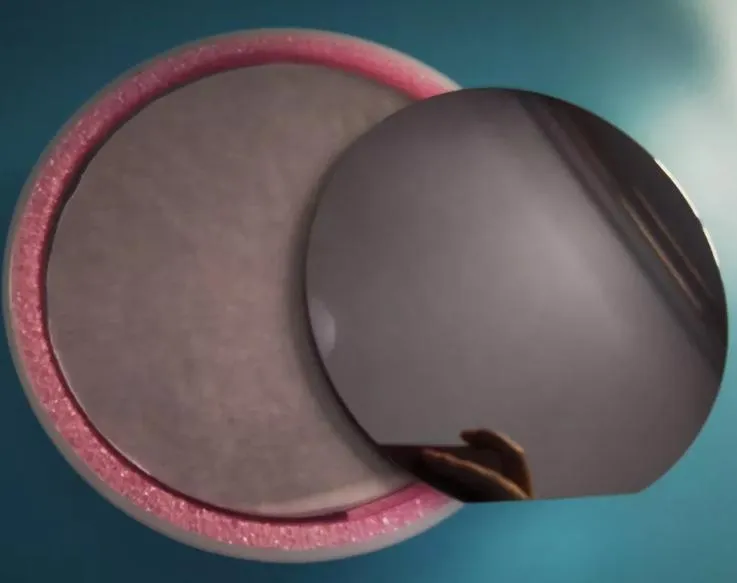
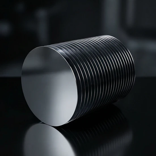
Packaging options: FOUP (Front Opening Unified Pod, 25 wafers), nitrogen-purged single-wafer shippers, vacuum-sealed multi-wafer cassettes
-
Shelf life: 24 months in unopened FOUP under Class 1 cleanroom environment
3. Core Industrial Applications
-
Primary industries: Logic device fabs (leading-edge nodes), DRAM manufacturers (≥1α), NAND flash producers (≥200+ layers), foundries (TSMC, Samsung, SMIC comparable specs)
-
Operational use cases:
-
EUV lithography patterning layers
-
Gate-all-around (GAA) FET and FinFET channels
-
High-bandwidth memory (HBM) interposer base
-
RF-SOI and power management ICs (with tailored resistivity)
-
-
Performance advantage: Lower oxygen precipitation variability (≤5%) vs. standard 300mm wafers → superior gate oxide integrity and 15% higher probe-test yield in sensitive analog/mixed-signal blocks.
-
Cost advantage: Larger die-per-wafer reduces edge die loss (≤3% vs. 7–9% on 200mm), lowering effective cost per good die by 22–30% for high-volume designs.
4. Competitive Advantages
-
Quality consistency: Statistical process control (SPC) with Cpk ≥1.33 for TTV, bow, and particle count; 100% auto-optical inspection (AOI) + SEM review on sampling.
-
Supply reliability: Dual-source raw poly silicon and backup crystal growth sites (Asia + Europe) with 52-week rolling forecast commitment.
-
Logistics capability: Climate-controlled, ESD-safe shipping; real-time IoT-enabled FOUP tracking; <1% on-time delivery deviation (DIFOT >99%).
-
Price competitiveness: Tiered pricing for contract volumes (≥2,000 wafers/month) with index-linked raw material adjustment cap (max +8% annually).
-
Sustainability: 70% recycled DI water in polishing; zero landfill wafer scrap; carbon-neutral shipping option available via verified offsets.
-
Technical support: Full lot traceability (SEMI M1–M12 compliant), SPC data package with each shipment, and 24/7 process integration engineering support.
5. Commercial & Supply Information
-
Minimum Order Quantity (MOQ): 100 wafers (trial/prototype); 1,000 wafers (production)
-
BULK order threshold: 20 metric tons (approx. 24,700 wafers, including packaging weight)
-
Loading capacity: 14 metric tons per standard 20-ft container (approx. 17,300 wafers in FOUPs, palletized)
or
24 metric tons per 40-ft HC container (approx. 29,600 wafers)
Reviews
There are no reviews yet.