
Description
1. Product Overview
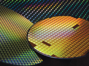
Wafer Backgrind Tape (BG Tape) is a high-performance, UV-curable or non-UV pressure-sensitive adhesive film engineered for wafer thinning processes in semiconductor backend manufacturing. Its primary industrial use is to protect the active circuit side of a silicon or compound semiconductor wafer during mechanical grinding and chemical etching to achieve ultra-thin die profiles. The key value proposition is a zero-defect reduction in wafer breakage, edge chipping, and die shifting—directly increasing backend yield by 3–7%. As device packaging moves toward 3D integration and stacked die architectures, BG Tape has become a strategically critical consumable for maintaining die strength and process reliability at sub-100µm wafer thicknesses.
2. Key Specifications & Technical Characteristics
-
Chemical Composition / Material Components:
-
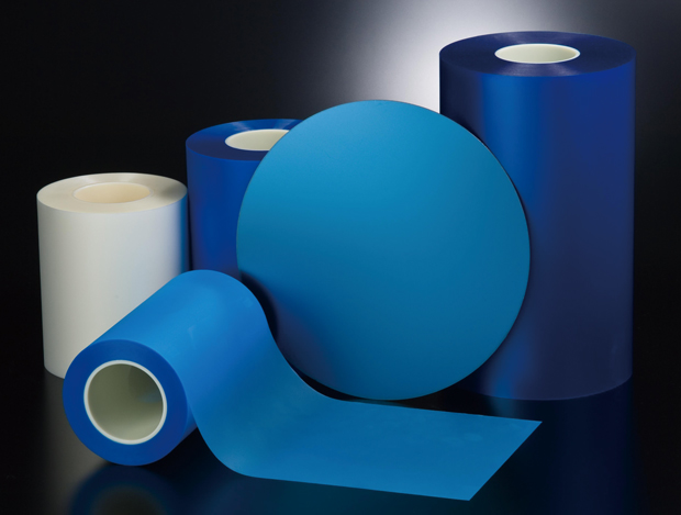
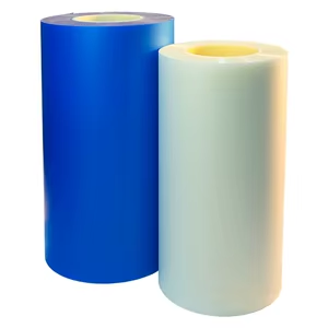
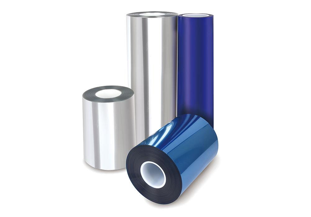
Base film: Polyolefin (PO) or PVC (standard) / PET-backing for ultra-thin wafers
-
Adhesive layer: UV-curable acrylic or rubber-based pressure-sensitive adhesive (PSA)
-
Release liner: Silicone-coated PET (50–75µm)
-
-
Purity Level / Grade:
-
Semiconductor grade (ISO Class 4–5 cleanroom manufactured)
-
Low outgassing (<0.5% total mass loss per ASTM E595)
-
Ionic impurity: Cl⁻ < 0.5 ppm, Na⁺ < 0.2 ppm, K⁺ < 0.2 ppm
-
-
Physical Characteristics:
-
Form: Single-sided tape with liner
-
Color: Translucent to light blue for edge detection
-
Total thickness: 90–160 µm (adhesive + film)
-
Adhesion strength (pre-UV): 150–250 gf/25mm (to Si)
-
Adhesion strength (post-UV, if UV type): <10 gf/25mm for easy debonding
-
Elongation at break: >400% (PO type)
-
-
Packaging Options:
-
Wafer frame mounted: 8″ or 12″ (300mm) pre-cut on ring
-
Roll format: 200–700mm width, 100–500m length
-
Individual die-level strips upon request
-
-
Shelf Life:
-
12 months from date of manufacture at 22±2°C / 50±10% RH (original sealed bag)
-
3. Core Industrial Applications
-
Primary industries: Semiconductor foundries, OSATs (outsourced semiconductor assembly and test), IDMs (integrated device manufacturers), MEMS manufacturers, power device fabs.
-
Specific operational use cases:
-
Wafer thinning from 750µm to 30–100µm for memory stacks (NAND, DRAM) and logic devices
-
Backside metal deposition protection during backgrind processes
-
Carrier tape replacement in temporary bonding/debonding workflows
-
-
Why this product performs better than alternatives:
-
Anti-static control: Surface resistivity <1×10¹¹ Ω/sq prevents die damage from charge accumulation—critical for CMOS and RF devices.
-
Edge ring protection: Proprietary adhesive anchoring reduces silicon residue contamination on grinder chuck tables, extending equipment maintenance cycles by 40%.
-
Low debris peel: Post-UV release leaves <0.1% adhesive residue vs. 2–5% on standard PVC tapes, eliminating wet cleaning steps.
-
Cost advantage: Polyolefin film absorbs grinding stress better than PET, allowing use of lower-cost finer grit wheels without edge chipping—reducing total consumable cost by 12–18%.
-
4. Competitive Advantages
-
Quality consistency: Cpk > 1.33 for adhesion, thickness, and particle count (≥0.3µm particles <50 per m²). Each lot ships with a certificate of analysis (CoA) and 3D surface profilometry report.
-
Supply reliability: Dual manufacturing sites (Asia and Europe) with 6-month rolling safety stock. Lead time: 15 days ARO for standard SKUs; 72-hour expedite available.
-
Logistics capability: Temperature-controlled cleanroom logistics chain with real-time IoT humidity/temp tracking. Direct line-feed to Class 1000 or better wafer fabs.
-
Price competitiveness: Volume pricing at 15–22% below leading Japanese and Korean Tier-1 brands for equivalent electrical and mechanical specs. No prepayment premium for qualified OEMs.
-
Sustainability & environmental benefits: PVC-free formulations available (100% incineration-compatible). Reel cores and packaging are 100% recycled cardboard. Carbon-neutral shipping option via verified emission offsets.
-
Technical support: Full UV wavelength (365nm / 254nm) dose mapping for your specific grinder model. On-site application engineering for tape expansion, mounting automation, and peel-angle optimization included with annual contracts.
5. Commercial & Supply Information
-
Minimum order quantity (MOQ):
-
5,000 wafer frames (8″ or 12″ pre-cut on ring)
-
OR 10 standard rolls (200mm × 200m equivalent)
-
-
BULK 20MT loading capacity:
One 20-foot dry container (20MT) = approx. 1,200,000 linear meters of 300mm-wide BG Tape, equivalent to ~400,000 units of 12″ wafer frames -
Loading capacity per container:
-
20FT standard container: 20 metric tons net (18 pallets, 48”×40” each)
-
40FT HC container: 22 metric tons net (36 pallets) – preferred for multi-SKU orders (e.g., 8″ + 12″ + UV + non-UV mixes)
-
Reviews
There are no reviews yet.