


Description
1. Product Overview
Photolithography Chemicals are high-purity specialty chemicals essential for semiconductor and microelectronics manufacturing. They enable precise patterning on silicon wafers, facilitating the fabrication of integrated circuits with nanometer-scale accuracy. These chemicals offer unmatched process reliability and uniformity, ensuring optimal yield and device performance. Strategically, they are critical in supporting advanced semiconductor production, making them indispensable for leading-edge electronics manufacturers. Their consistent quality and industrial-grade formulation provide a competitive edge for suppliers and buyers in the global semiconductor supply chain.
2. Key Specifications & Technical Characteristics
- Chemical Composition: Proprietary photoresists, developers, etchants, and solvents tailored for photolithography processes
- Purity Level: Semiconductor-grade, >99.9% purity where applicable
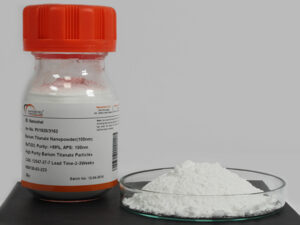
- Physical Characteristics: Available in liquid, solution, or powder form; clear to light-colored appearance; particle-free formulations
- Packaging Options: Industrial drums (5–200 L), ISO tanks for bulk liquids, sealed high-purity containers
- Shelf Life: Typically 12–24 months under recommended storage conditions; temperature-controlled storage advised
3. Core Industrial Applications
- Primary Industries: Semiconductor fabrication, MEMS devices, advanced PCB manufacturing, microelectronics research and development
- Operational Use Cases:
- Photoresist application and pattern transfer on silicon wafers
- Etching and cleaning processes during chip fabrication
- Precision coating and development for micro- and nano-scale circuitry
- Performance Advantages: High chemical stability, low contamination risk, and superior adhesion and resolution enhance process efficiency, yield consistency, and cost-effectiveness compared to generic chemical alternatives
4. Competitive Advantages
- Quality Consistency: Rigorous quality control ensures batch-to-batch uniformity
- Supply Reliability: Scalable production and global logistics network minimize downtime risk
- Technical Support: Comprehensive documentation and process guidance available
- Price Competitiveness: Bulk purchasing options optimize cost per wafer
- Sustainability: Compliance with environmental and semiconductor industry standards, including reduced hazardous waste generation
5. Commercial & Supply Information
- Minimum Order Quantity (MOQ): BULK 20 MT
- Loading Capacity: Up to 20 MT per 20-foot container, with specialized packaging to prevent contamination

Reviews
There are no reviews yet.