
Description
1. Product Overview
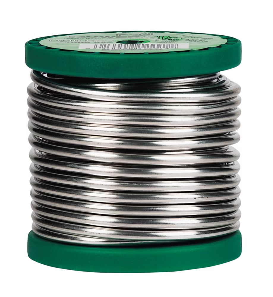
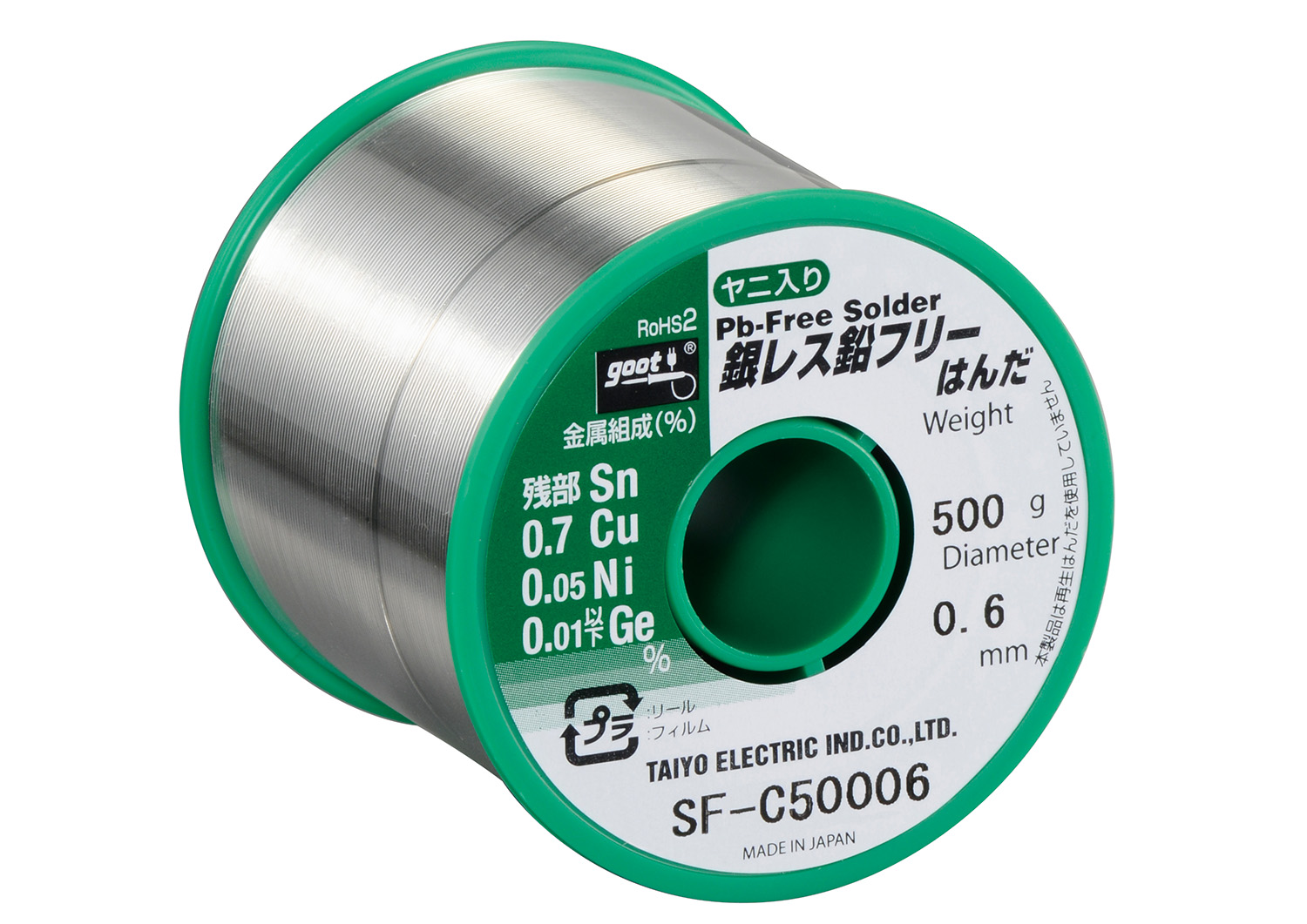
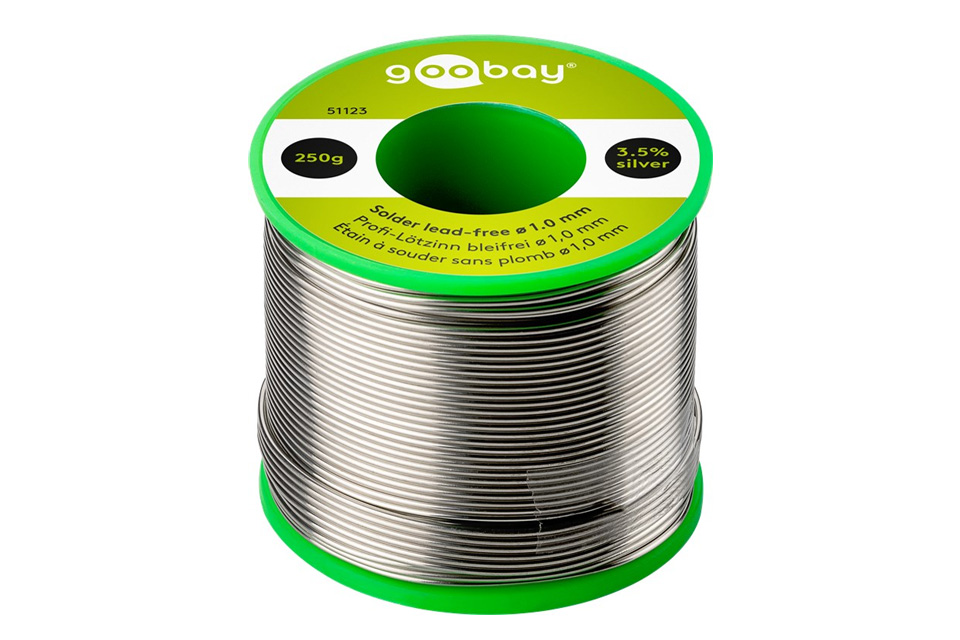
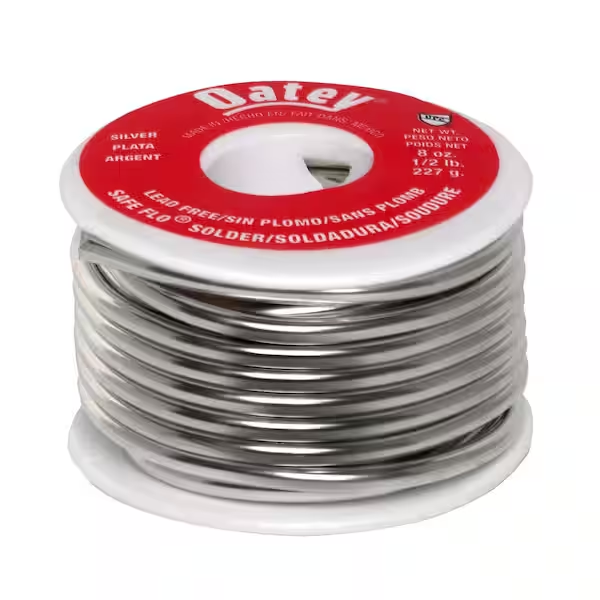
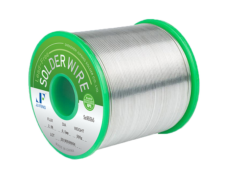
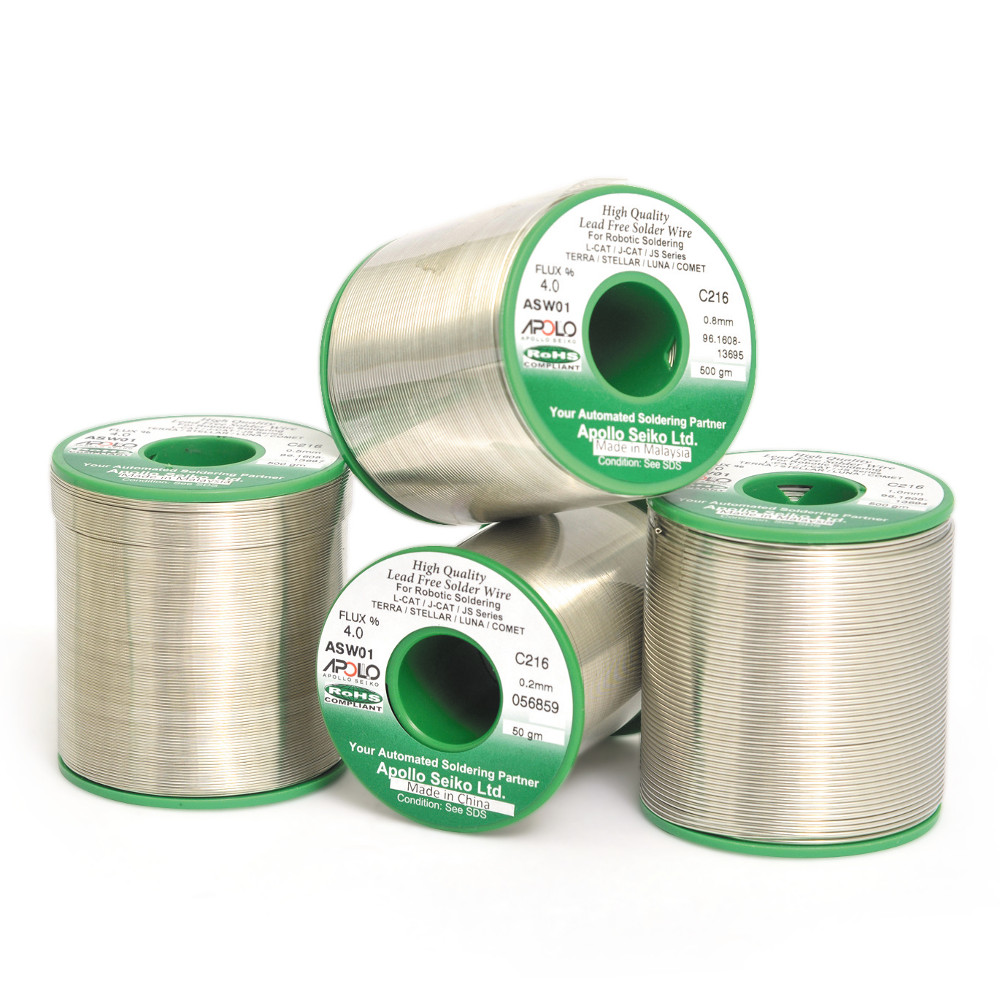
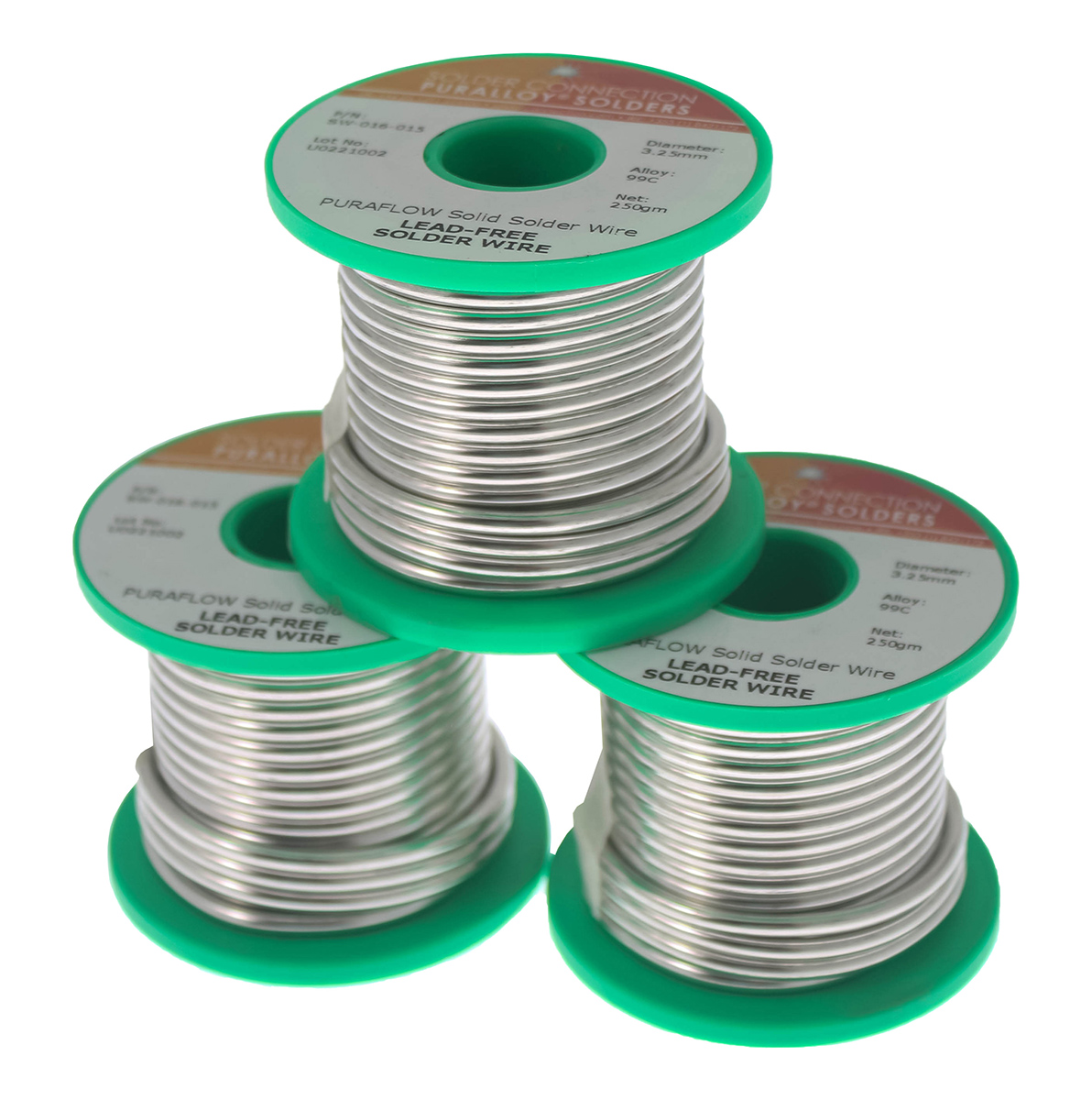
Lead-Free Solder is a high-performance, environmentally compliant solder alloy designed for precision joining of metals in industrial and electronics manufacturing. Engineered to meet rigorous international standards, it ensures reliable electrical conductivity and strong mechanical bonding while eliminating lead-related health and environmental risks. Its strategic importance lies in supporting global regulatory compliance (RoHS, WEEE) and enabling manufacturers to deliver safer, high-quality electronic and industrial assemblies. With superior flow characteristics, thermal stability, and long-term durability, this solder enhances operational efficiency and reduces rework in high-volume production environments.
2. Key Specifications & Technical Characteristics
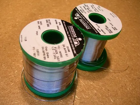
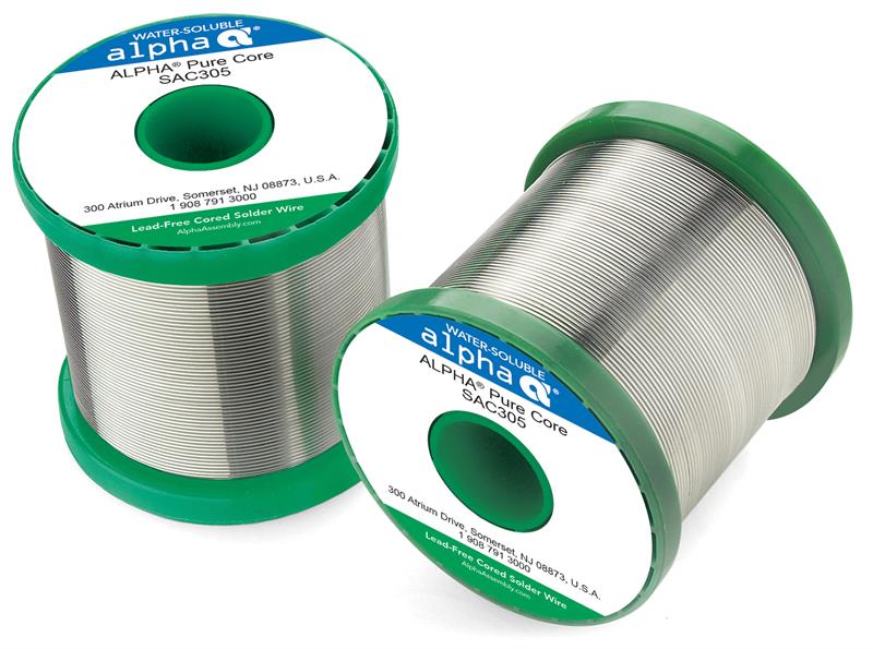
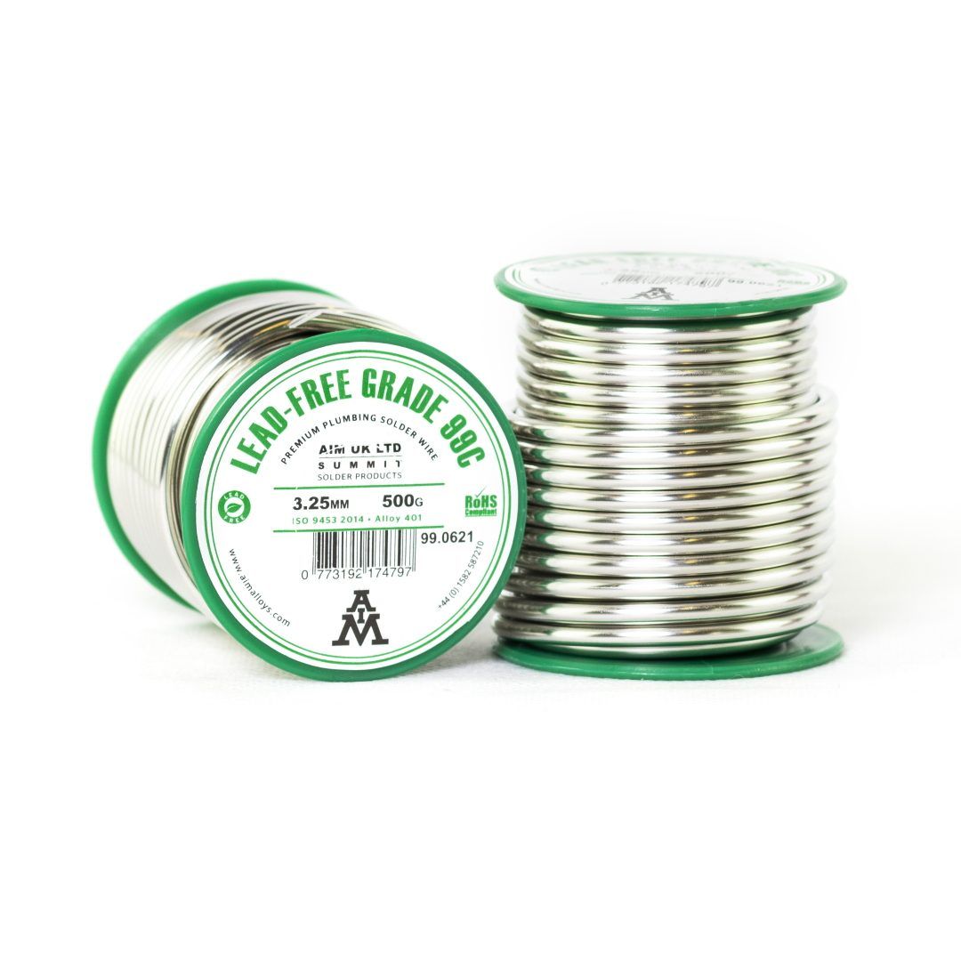
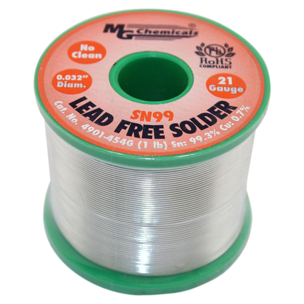
- Chemical Composition: Tin (Sn) 99.3%, Copper (Cu) 0.7% — standard SnCu formulation
- Purity Level / Grade: Industrial-grade, ≥99.3% purity
- Physical Form: Wire, spool, or pellet
- Color: Silver-gray metallic
- Melting Point: 227–230 °C
- Diameter / Particle Size: 0.5 mm, 1 mm, 1.5 mm (wire); customizable pellets available
- Density: 7.3 g/cm³
- Packaging Options: 500 g, 1 kg, 5 kg spools; 10 kg, 20 kg bulk boxes
- Shelf Life: 24 months under recommended storage conditions (cool, dry, away from moisture)
3. Core Industrial Applications
- Primary Industries: Electronics manufacturing, automotive, aerospace, renewable energy, precision instrumentation
- Operational Use Cases: PCB assembly, component mounting, electrical wiring, metal joining in precision equipment
- Performance Advantages:
- Eliminates lead-related contamination and health hazards
- Superior wetting and flow for consistent solder joints
- Enhanced thermal stability reduces voids and cracking
- Optimized for high-speed automated soldering processes
This product delivers reliable joint integrity, reduces defect rates, and supports sustainable manufacturing practices, making it the preferred choice over traditional leaded solders.
4. Competitive Advantages
- Quality Consistency: Rigorous quality control ensures uniform alloy composition and performance across batches
- Supply Reliability: Global manufacturing and logistics network ensures steady availability for high-volume industrial buyers
- Technical Support: Comprehensive datasheets, process guidance, and consultation services available
- Price Competitiveness: Cost-effective solution compared to other high-purity, lead-free alternatives
- Sustainability & Environmental Benefits: Fully RoHS-compliant, minimizing regulatory risk and environmental impact
5. Commercial & Supply Information
- Minimum Order Quantity (MOQ): 20 MT
- Loading Capacity: 20 MT per standard 20 ft container
- Delivery: Flexible logistics options with bulk shipping support for industrial clients


Reviews
There are no reviews yet.