
Description
1. Product Overview
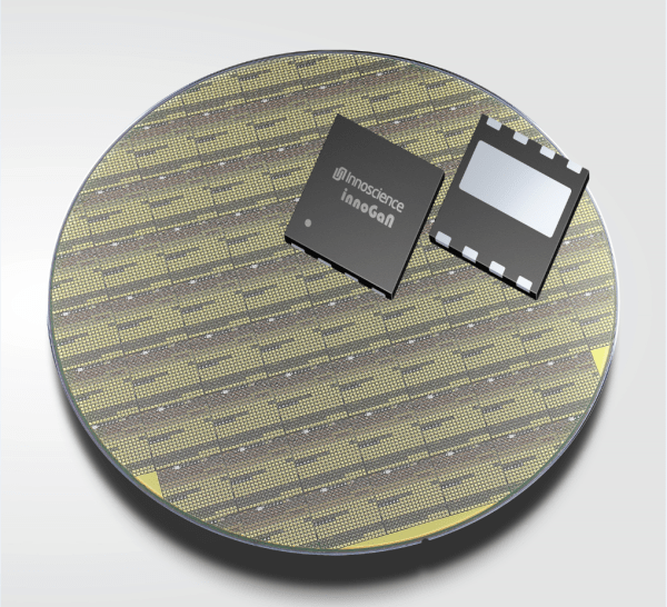
This product is a high-performance Gallium Nitride on Silicon (GaN-on-Si) epitaxial wafer, engineered for next-generation power electronics and RF semiconductor devices. It is primarily used in high-voltage power conversion systems, 5G infrastructure base stations, and fast-charging solutions. The key value proposition lies in its ability to deliver superior energy efficiency, higher switching frequencies, and lower thermal resistance compared to traditional silicon—while leveraging existing silicon foundry infrastructure for cost scalability. Strategically, GaN-on-Si is critical for enabling global decarbonization goals and reducing energy loss in data centers, EVs, and industrial motors.
2. Key Specifications & Technical Characteristics
-
Chemical Composition / Material Stack: Si(111) substrate / AlN nucleation layer / AlGaN buffer layer / GaN channel / AlGaN barrier / GaN cap
-
Purity Level: Transition metal impurity < 1E10 atoms/cm²; surface particle count ≤ 0.05 particles/cm² (≥0.3µm)
-
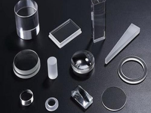
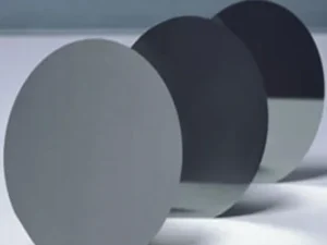
Physical Characteristics:
-
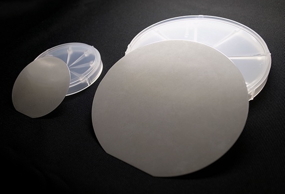
Wafer diameter: 150mm (6”) or 200mm (8”)
-
Thickness: 1,000 µm ± 25 µm (substrate); epi thickness 5–6 µm
-
Bow/Warp: ≤ 40 µm / ≤ 60 µm
-
Surface roughness (RMS): ≤ 0.5 nm (5×5 µm AFM)
-
-
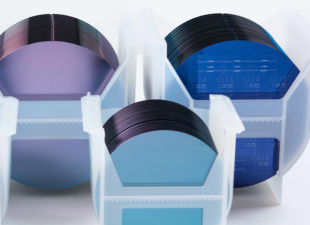
Packaging Options: Single-wafer FOUP (Front Opening Unified Pod) or multi-wafer H-bar cassettes; nitrogen-purged vacuum-sealed containers.
-
Shelf Life: 12 months from ship date when stored in original sealed packaging at 20–25°C / 30–50% RH; avoid UV exposure.
3. Core Industrial Applications
-
Primary Industries: Electric vehicles (on-board chargers & DC-DC converters), telecom infrastructure (5G massive MIMO), data center power supplies, industrial motor drives, consumer fast chargers (>100W).
-
Specific Operational Use Cases:
-
48V–800V DC-DC converters for EVs: reduces switching loss by 70% vs Si MOSFETs.
-
5G RF power amplifiers: enables 6.8 GHz operation with 65% PAE (power-added efficiency).
-
-
Why Better Than Alternatives: GaN-on-Si operates at 2–5x higher frequency and 3x lower output capacitance than silicon. Compared to SiC, GaN-on-Si costs 40% less at similar voltage ratings (650V class). Unlike bulk GaN, GaN-on-Si allows 200mm fab scalability, lowering per-die cost.
4. Competitive Advantages
-
Quality Consistency: Statistical process control with ≤ 1.5 Cpk for sheet resistance and 2DEG mobility (≥2,000 cm²/V·s). 100% automated optical inspection and X-ray diffraction mapping on every wafer.
-
Supply Reliability: Dual-source epitaxy lines (Taiwan and Germany) with 4-week standard lead time; 99.3% on-time delivery rate over 24 months.
-
Logistics Capability: Global hub shipping from Rotterdam, Singapore, and Los Angeles; fully insured climate-controlled transport.
-
Price Competitiveness: Tiered pricing starting 15–20% below market average for annual volumes >5,000 wafers.
-
Environmental & Technical Support: Full RoHS, REACH, and conflict mineral compliance. Included: epitaxy structure simulation file (Sentaurus TCAD), failure analysis hotline (24h response), and qualification package for JEDEC JEP180.
5. Commercial & Supply Information
-
Minimum Order Quantity (MOQ): 25 wafers (engineering grade) or 500 wafers (production grade)
-
BULK 20MT Loading Capacity (per container): Not applicable (wafer count density). Instead:
-
Max wafer quantity per 20’ container: 120,000 units (150mm wafers in FOUPs; palletized)
-
Equivalent MT: Approx. 1.2 metric tons (wafer mass only) per 20’ container
-

Reviews
There are no reviews yet.