
Description
1. Product Overview
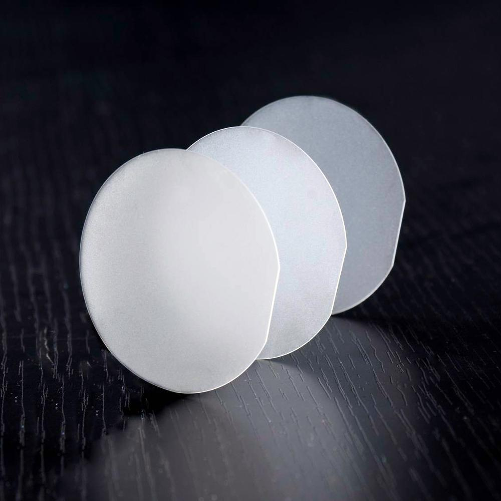
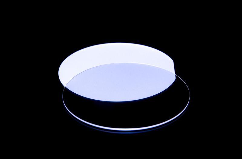
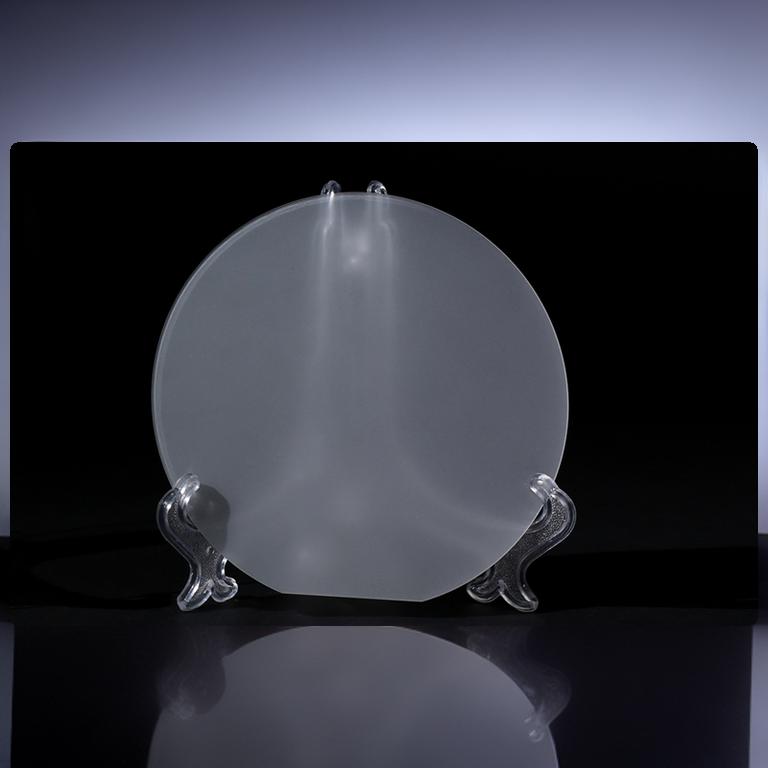
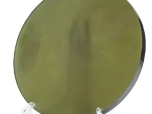
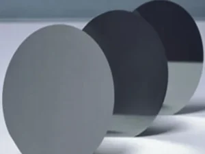
The 2-Inch C-Plane Sapphire Wafer is a precision-engineered single-crystal aluminum oxide (Al₂O₃) substrate, manufactured for epitaxial thin-film deposition in high-performance semiconductor and optical devices. Its primary industrial use lies in serving as the foundational template for Gallium Nitride (GaN) LED epitaxy, RF filters, and power electronics. The key value proposition is its atomically flat C-plane orientation, which delivers unmatched lattice-matching efficiency for GaN growth, directly translating to higher device yield and lower defect densities. Strategically, as global demand for energy-efficient lighting, 5G communications, and electric vehicle power modules accelerates, reliable C-plane sapphire wafers remain a non-negotiable bottleneck enabler for the wide-bandgap semiconductor supply chain.
2. Key Specifications & Technical Characteristics
-
Chemical Composition: Single-crystal Al₂O₃ (Sapphire), 99.999% (5N) purity
-
Crystal Orientation: C-Plane (0001) ± 0.2°, with primary flat orientation (A‑plane) per SEMI standards
-
Diameter: 50.8 mm (2 inches) ± 0.1 mm
-
Thickness: 430 µm ± 25 µm (custom 330–1000 µm available)
-
Surface Finish: Epitaxy-ready, CMP-polished
-
Ra ≤ 0.2 nm (AFM, 10×10 µm²)
-
Microroughness: < 0.1 nm RMS
-
-
TTV (Total Thickness Variation): ≤ 5 µm
-
Bow / Warp: ≤ 10 µm / ≤ 15 µm
-
Edge Chipping: ≤ 100 µm (no chips > 0.5 mm depth)
-
Laser Marking: Optional SEMI-standard alphanumeric (backside, non-patterned area)
-
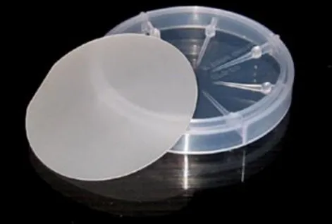
Packaging: Single-wafer PET film separated, in class 10 cleanroom cassette or single-wafer containers, vacuum-sealed with nitrogen purge
-
Shelf Life: 24 months when stored in original packaging at 20–25°C, < 40% humidity
3. Core Industrial Applications
-
Primary Industry: High-brightness LED (HB-LED) manufacturing for general lighting, automotive, and display backlighting.
-
Specific Operational Use Cases:
-
MOCVD (Metal-Organic Chemical Vapor Deposition) of GaN blue/green LED epilayers.
-
Production of surface acoustic wave (SAW) filters for 5G front-end modules.
-
Substrates for power Schottky diodes and GaN-on-Si emergency RF devices.
-
-
Why This Product Performs Better than Alternatives:
-
Superior lattice match (misfit ~16% vs. Si ~41%) reduces threading dislocation density (TDD < 5×10⁶ cm⁻²) vs. silicon substrates, directly boosting LED external quantum efficiency by 8–12%.
-
Ultra-low micropipe density (zero) compared to SiC wafers, eliminating yield-killing substrate-induced breakdown in power devices.
-
High thermal conductivity (35 W/m·K) and chemical inertness enable higher MOCVD temperatures (up to 1200°C) without degradation – unlike glass or Si alternatives.
-
-
Cost Advantage per Die: Lower defect density enables larger LED chip sizes (1×1 mm²) with same yield, reducing per-lumen cost by ~15% vs. standard C-plane wafers with higher TTV.
4. Competitive Advantages
-
Quality Consistency: Each production lot undergoes 100% automated optical inspection (AOI), laser interferometry for TTV/Bow, and AFM spot checks. Certificate of Analysis (CoA) includes full metrology traceable to NIST standards.
-
Supply Reliability: Dual-source crystal ingot agreement (Kyropoulos and EFG methods) with > 25,000 wafers/month capacity. Safety stock held in three regional hubs (NA, EU, APAC).
-
Logistics Capability: Ex-works, FCA, CIF delivery options. Temperature-controlled, shock-indicator-tagged packaging available for air or sea freight.
-
Price Competitiveness: Tiered pricing based on annual commitment (1K, 5K, 20K+ pieces). Volume pricing lower than incumbent Japanese suppliers by 8–10% with identical or tighter TTV specs.
-
Sustainability: 60% of input Al₂O₃ from recycled LED scrap; manufacturing water recycled at 85% closed-loop; RoHS 3 and REACH compliant.
-
Technical Support: Free pre-sale epitaxy qualification (up to 10 wafers). Post-sale process integration engineering included for orders > 500 units.
5. Commercial & Supply Information
-
Minimum Order Quantity (MOQ): 20 pieces (epi-ready, single-side polished C-plane)
-
Bulk 20MT Loading Capacity: Not applicable – wafer product. Equivalent: Maximum 12,000 wafers per standard export carton pallet (20 pallets per 20’ container = 240,000 wafers per 20’ container)
-
Standard Lead Time: 14 days for MOQ; 28 days for full container load (240K units)
-
Incoterms Offered: EXW (Singapore factory), FOB (Singapore), CIF (major global airports/seaports)
-
Payment Terms: L/C at sight (for orders > $50k) or net 30 days for approved corporate accounts
Reviews
There are no reviews yet.