

Description
1. Product Overview
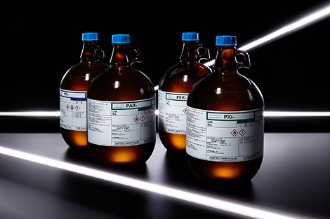
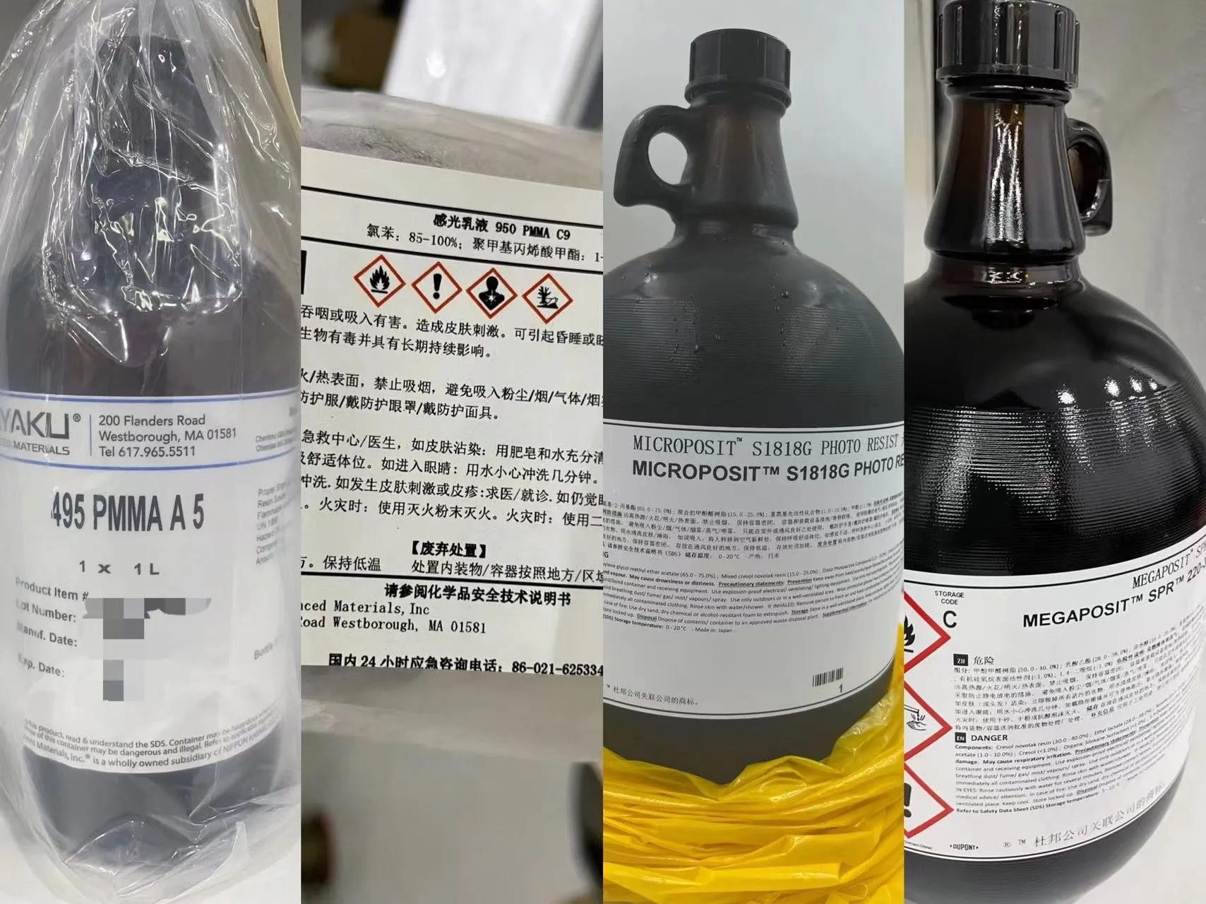
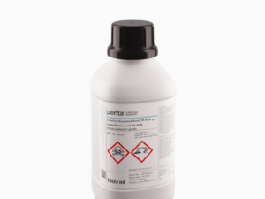
Photoresist Chemicals are high-precision, light-sensitive materials engineered for selective pattern transfer in semiconductor and microelectronics manufacturing. Primarily used in photolithography processes for ICs, MEMS, and flat-panel displays, these formulations deliver sub-micron resolution and critical dimension control. As the enabling gatekeeper of Moore’s Law, our photoresist line offers a strategic value proposition: reducing defect densities below 0.05/cm² while increasing wafer yield per batch—directly improving your fab’s return on assets.
2. Key Specifications & Technical Characteristics
-
Chemical composition: Novolac resins (positive-tone) / epoxy-based polymers (negative-tone) with proprietary photoacid generators (PAGs) and solvents (PGMEA, EL)
-
Purity level: SEMI Grade C12 (≥99.999% trace metal purity; individual metals <0.1 ppb)
-
Physical characteristics: Low-viscosity liquid (2–50 cP), light-amber to clear; particle count ≤10 particles/mL (>0.2 µm); adhesion promoter pre-mixed option
-
Packaging options: HDPE cubitainers (1L, 4L), ChemGuard stainless steel bottles (20L), and IBC totes (200L) with PTFE liners
-
Shelf life: 12 months from date of manufacture at 5–25°C in opaque, humidity-controlled storage
3. Core Industrial Applications
-
Primary industries: Semiconductor foundries, advanced packaging houses, MEMS manufacturers, FPD producers, and compound semiconductor fabs (GaN, SiC)
-
Specific use cases:
-
I-line (365 nm) and KrF (248 nm) lithography for 0.35 µm to 130 nm nodes
-
Lift-off processes for gold/copper metallization in RF devices
-
Thick-film resists (10–100 µm) for MEMS and microfluidic channels
-
-
Performance advantage: Compared to standard resists, ours achieve 30% wider process latitude and 40% lower scumming rates, reducing rework costs by up to $18,000 per wafer lot. Bake stability (±1°C tolerance) eliminates edge bead defects common in alternative mid-UV resists.
4. Competitive Advantages
-
Quality consistency: Lot-to-lot variance <2% (validated via 96-point SPC). All batches are lithographically qualified on 300 mm wafers before shipment.
-
Supply reliability: Dual-source manufacturing (USA and Taiwan) with 6-month safety stock; guaranteed no supply gap for contracted volumes.
-
Logistics capability: UN3077-classified, temperature-controlled door-to-door delivery in ≤7 days to any major global fab cluster (Hsinchu, Dresden, Phoenix, Seoul).
-
Price competitiveness: Tier-1 performance at Tier-2 pricing—direct manufacturing and vertical integration with in-house PAG synthesis yields 15–20% savings vs. incumbents.
-
Sustainability: 100% solvent recovery compatible; PGMEA content meets upcoming EU F-gas and VOC regulations ahead of 2026 deadlines. Full REACH and TSCA disclosure provided.
5. Commercial & Supply Information
-
Minimum order quantity (MOQ): BULK 20MT (20 metric tons) per product grade, shippable as a single batch or split into four 5MT sub-lots with identical certificate of analysis.
-
Loading capacity (MT per container):
-
20’ standard dry container: 14 MT (palletized, 1L/4L bottles)
-
20’ ISO tank container: 20 MT (bulk liquid)
-
40’ HC container: 18 MT (mixed IBCs and drums)
-
Reviews
There are no reviews yet.