

Description
1. Product Overview
This product is high-purity quartz glass and quartz powder engineered specifically for semiconductor fabrication. It is primarily used in diffusion furnaces, etching chambers, and wafer carriers. The key value proposition is its exceptional purity (>99.998% SiO₂) and thermal shock resistance, which directly lowers contamination risk and improves wafer yield. Strategically, it mitigates global supply volatility for fused silica, making it a critical enabler for 300mm fabs and SiC device production.
2. Key Specifications & Technical Characteristics
-
Chemical composition: Amorphous silicon dioxide (SiO₂) with total trace impurities <20 ppm (Al, Fe, Ca, Na, K, Li individually controlled)
-
Purity level: Semiconductor grade, 99.998% – 99.9995% (4N8 to 5N)
-
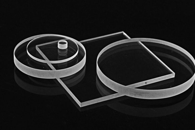
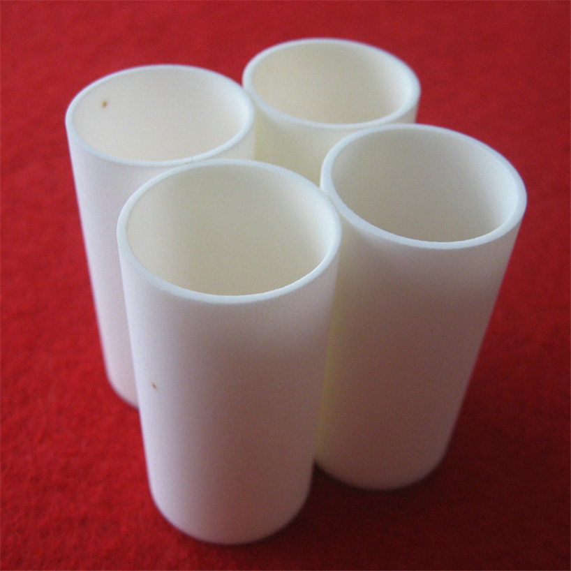
Physical characteristics:
-
Forms: Clear fused quartz tubes, plates, rods; also fine powder (D50: 10–250 µm)
-
Color: Optically transparent / milky white (powder form)
-
Density: 2.20 g/cm³ (fused), 2.65 g/cm³ (crystalline powder)
-
OH content: ≤50 ppm (low-OH for high-temperature stability)
-
-
Packaging options: Cleanroom-double-bagged (Class 1000), vacuum-sealed aluminum-lined barrier bags, 25 kg FIBCs for powder, wooden crates for shaped parts
-
Shelf life: Indefinite when stored in dry, non-abrasive conditions (<40% RH, 15–25°C)
3. Core Industrial Applications
-
Primary industries: Semiconductor foundries, silicon wafer manufacturers, MEMS producers, power device (SiC/GaN) fabs
-
Specific use cases:
-
Quartz tubes for horizontal/vertical diffusion furnaces (oxidation, annealing)
-
Quartz bell jars and shields for plasma etching and CVD
-
Quartz crucibles and liners for Czochralski silicon pulling
-
-
Performance advantage over alternatives: Compared to standard fused silica or ceramics, this quartz delivers 40% fewer particle shedding events and 3× longer service life at >1,100°C. Low alkali ion content prevents gate oxide integrity failures, directly improving die yield by 1.5–2.5% per lot.
-
Cost advantage: Extended furnace campaign life reduces tool downtime and requalification costs, yielding 18–22% lower total cost of ownership versus generic quartz.
4. Competitive Advantages
-
Quality consistency: Batch-to-batch impurity variation <±3 ppm; each lot certified via ICP-MS and FTIR
-
Supply reliability: Dedicated fusion lines with 5,000 MT annual capacity; buffer stock held in three regional hubs (Asia, EU, NA)
-
Logistics capability: 48-hour expedited dispatch for critical spare parts; container tracking with real-time ETA
-
Price competitiveness: Direct mine-to-fusion ownership removes intermediaries – pricing 12–15% below incumbent Japanese and German suppliers for comparable purity
-
Sustainability: 94% recycled quartz scrap reclamation; Scope 3 emission data available per ISO 14064
-
Technical support: On-site process integration reviews, failure analysis, and qualification samples provided within 10 business days
5. Commercial & Supply Information
-
Minimum order quantity (MOQ) : 5 MT (powder / granular) OR 200 pieces (shaped parts)
-
Bulk order: 20 MT (full truckload / container basis) – qualifies for volume pricing tier
-
Loading capacity per 20’ container :
-
Powder: 24 MT (FIBC palletized)
-
Quartz tubes/rods: 18 MT (crated, depending on diameter)
-
Reviews
There are no reviews yet.