
Description
1. Product Overview
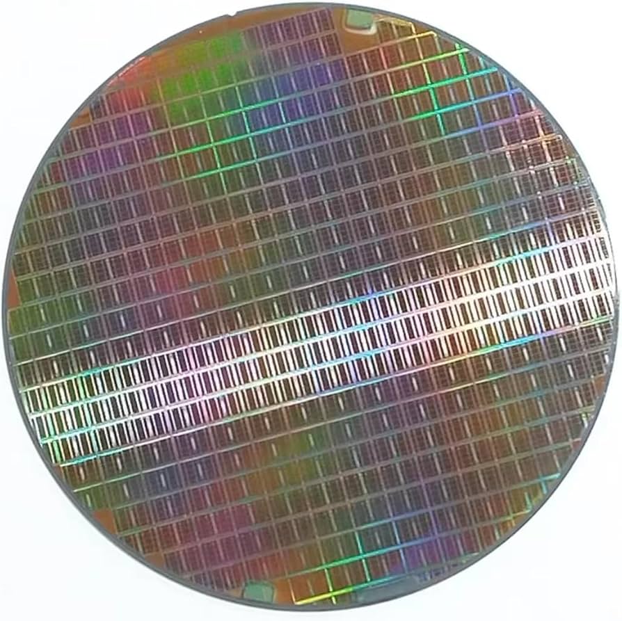
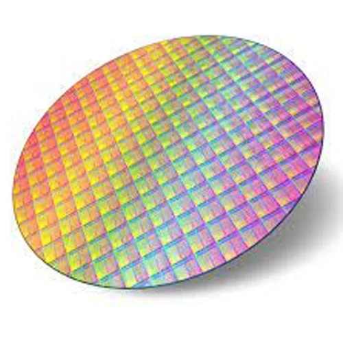
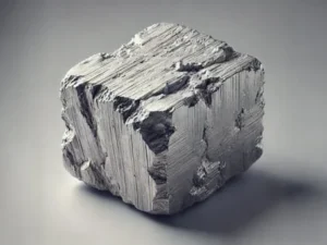
Semiconductor wafers are high-purity, single-crystal substrates—primarily silicon—engineered as the foundational layer for microelectronics and integrated circuits (ICs). They serve as the critical starting material for chip fabrication across computing, telecommunications, and power management systems. The core value proposition lies in their atomic-level flatness, minimal defect density, and batch-to-batch electrical uniformity, which directly enable advanced node lithography and device yield optimization. Strategically, they are the structural backbone of the global digital economy, where wafer quality determines semiconductor performance, energy efficiency, and manufacturing profitability.
2. Key Specifications & Technical Characteristics
-
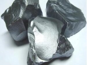
Chemical composition: Single-crystal silicon (Si), optionally doped with boron (p-type) or phosphorus (n-type); or compound III-V variants (GaAs, InP) upon request
-
Purity level: 99.9999999% (9N–11N) for silicon; metals content <0.1 ppb per element
-
Physical characteristics:
-
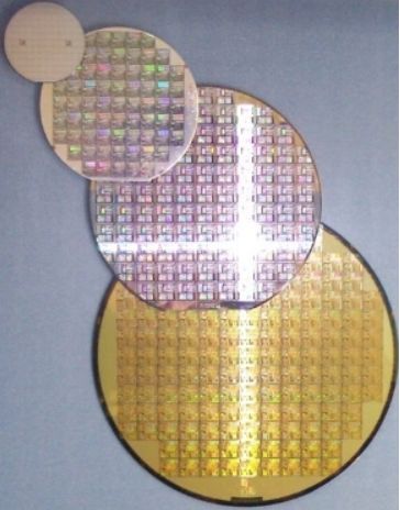
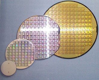
Diameters: 150mm, 200mm, 300mm (mass production); 450mm capability under development
-
Crystal orientation: Primarily <100> or <111> (±0.5°)
-
Thickness: 525 µm – 775 µm (depending on diameter)
-
Bow/warp: <30 µm, TTV (total thickness variation) <2 µm
-
Surface finish: Polished (SSP), double-side polished (DSP), or epitaxial layer (epi-ready)
-
-
Packaging options: Single-wafer FOUP (front opening unified pod), multi-wafer shipping cassettes (25 wafers), vacuum-sealed nitrogen-purged containers
-
Shelf life: >24 months when stored in inert atmosphere (N₂) at 18–25°C, <50% relative humidity
3. Core Industrial Applications
-
Primary industries: Semiconductor foundries (logic & memory), MEMS (micro-electro-mechanical systems), power device manufacturers, and optoelectronics
-
Specific use cases:
-
Logic & memory ICs: 7nm to 65nm node processors, DRAM, NAND flash
-
Power electronics: 200mm Si wafers for IGBTs and MOSFETs (EV charging, industrial motor drives)
-
MEMS: 150mm wafers for accelerometers, pressure sensors, microphones (automotive & consumer)
-
RF & optoelectronics: GaAs wafers for 5G front-end modules and VCSELs
-
-
Performance advantages over alternatives: Ultra-low defect density (≤0.1 defects/cm²) versus reclaimed or lower-grade wafers → 15–30% higher good-die-per-wafer yield. Tighter thickness/bow tolerances reduce photolithography alignment errors, enabling smaller feature sizes and lower parasitic capacitance.
4. Competitive Advantages
-
Quality consistency: 6-sigma process control (±3σ < 2% spec deviation) with full wafer-mapping metrology data (SEMI M1, M6, M20 compliant)
-
Supply reliability: Vertically integrated ingot pulling to polished wafer finishing; 100% laser-marked traceability; 98% on-time-in-full (OTIF) rate for blanket and test wafers
-
Logistics capability: Global hub stocking (Asia, EU, NA); direct line to fab C-free packaging; expedited 5-day delivery for engineering-grade wafers
-
Price competitiveness: Tiered pricing for prime, test, and monitor grades; volume discounts above 5,000 wafers/month; long-term supply agreements lock raw silicon costs
-
Sustainability: Up to 40% recycled silicon in non-critical grades; closed-loop slurry water recovery; carbon-neutral shipping option for EU buyers
-
Technical support: 24/6 process integration engineering support; incoming QC report with each batch; on-site audit and sampling program for strategic accounts
5. Commercial & Supply Information
-
Minimum order quantity (MOQ): BULK 20MT (approx. 6,000–8,000 wafers depending on diameter, cassette-packed)
-
Loading capacity (MT per container):
-
20FT standard container: 25 MT max (12 pallets / 240 cassettes) → recommend 22 MT net wafer mass for transport safety
-
40FT HC container: 28 MT max (26 pallets / 520 cassettes) → 26 MT net practical capacity
-
Note: Quantities include cassettes and FOUP weight; contact supply desk for case-specific cube-out optimization
-
Reviews
There are no reviews yet.