
Description
1. Product Overview
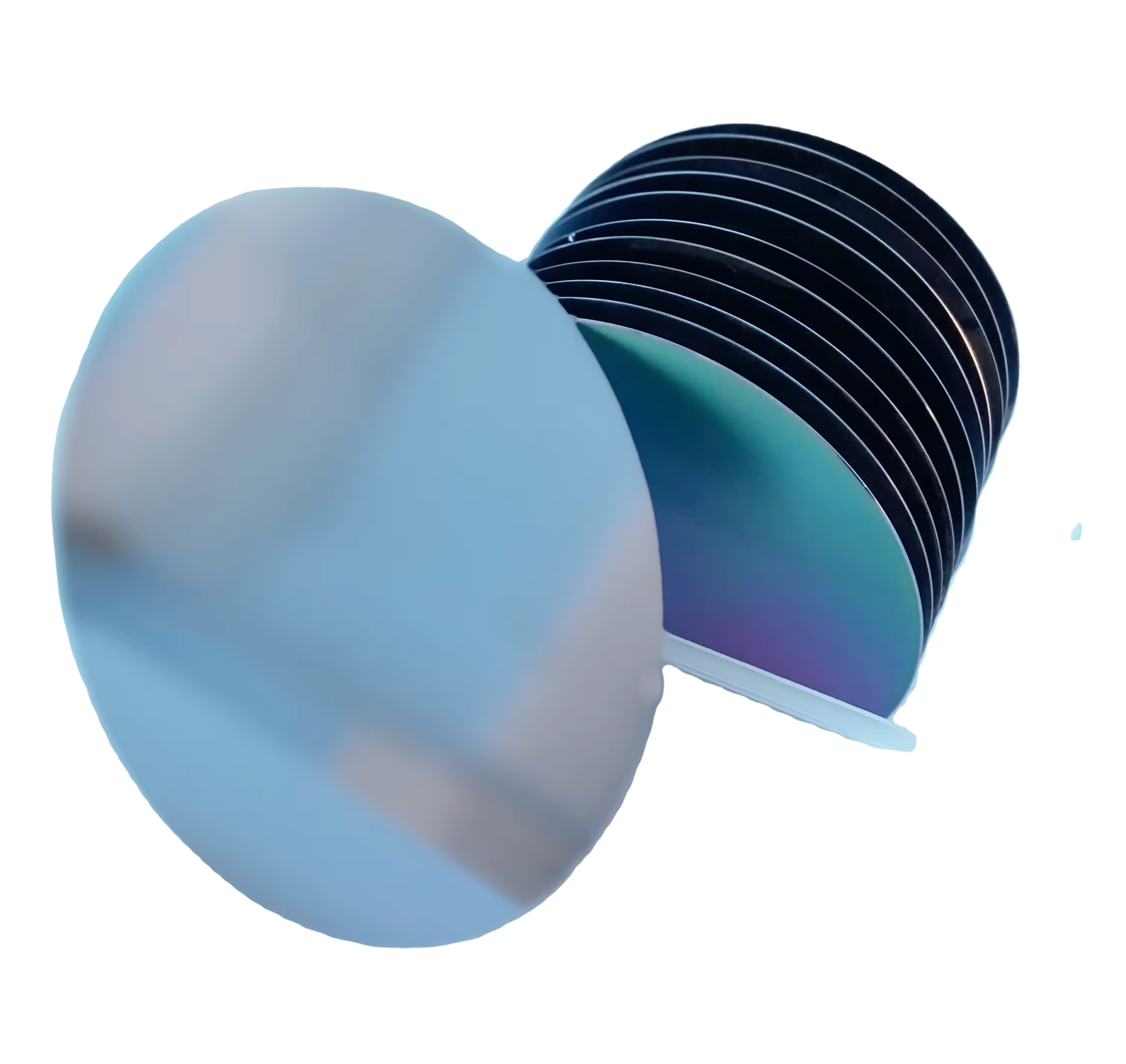
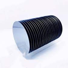
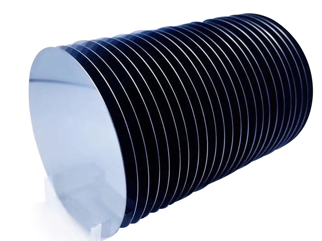
Silicon wafers are high-purity, crystalline substrates meticulously engineered for semiconductor and photovoltaic applications. They serve as the foundational material for integrated circuits, microelectronics, and solar cells, where precision and consistency are critical. These wafers offer unmatched structural integrity and electronic properties, ensuring optimal device performance and yield. Strategically, silicon wafers remain indispensable in global electronics and solar energy supply chains, making them a core component for manufacturers seeking reliable, high-performance materials. Their consistent quality and scalability make them a vital asset for industrial leaders worldwide.
2. Key Specifications & Technical Characteristics
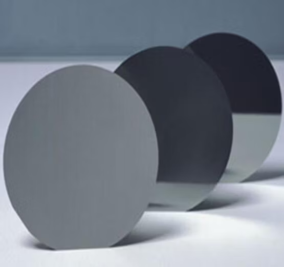
- Material Composition: Monocrystalline silicon (Si) or Polycrystalline silicon (Si)
- Purity Level: ≥ 99.9999% (6N) for semiconductor-grade; ≥ 99.99% (4N) for photovoltaic-grade
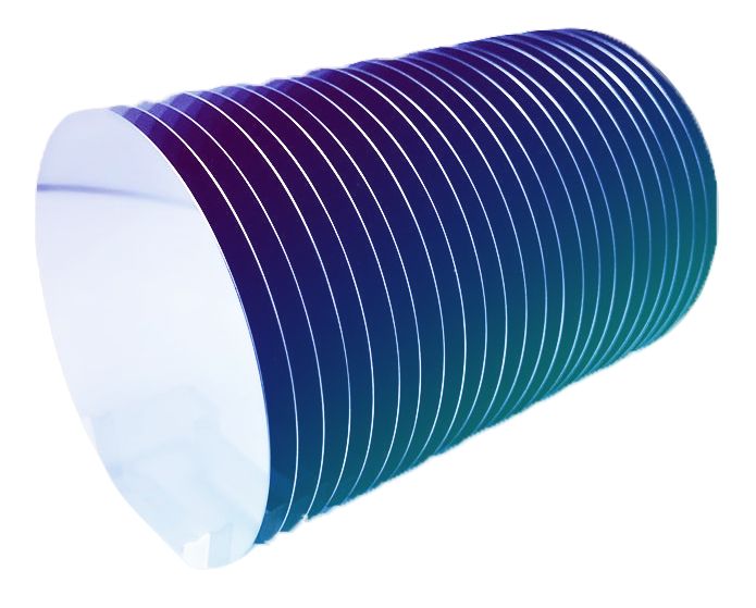
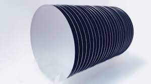
- Diameter Options: 50 mm – 300 mm standard wafers
- Thickness: 150 µm – 775 µm (customizable per industrial requirement)
- Surface Finish: Polished, lapped, or textured depending on application
- Crystallographic Orientation: <100>, <111> available
- Resistivity: 0.001 – 10 Ω·cm (application-specific)
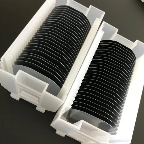
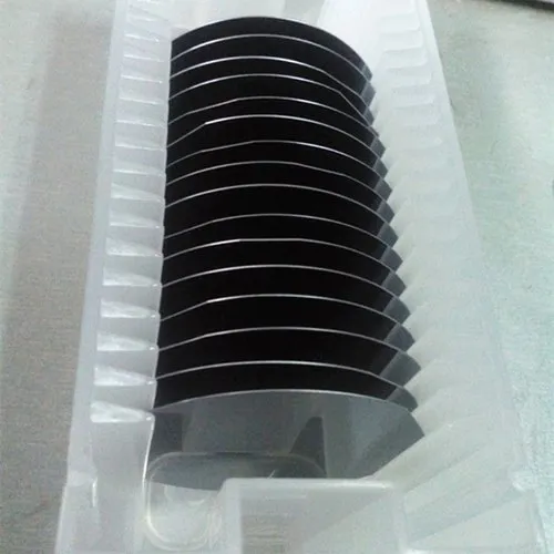
- Packaging: Anti-static trays, vacuum-sealed bags, or bulk crates for safe transport
- Shelf Life: Typically >24 months when stored under standard cleanroom conditions
3. Core Industrial Applications
- Semiconductor Industry: Substrate for ICs, microprocessors, memory chips, and sensors. Enables high-precision photolithography and doping processes.
- Photovoltaic Industry: Solar cell fabrication for large-scale renewable energy projects; high conversion efficiency due to superior crystalline structure.
- MEMS Devices: Micro-electromechanical systems in automotive, medical, and aerospace sensors.
- High-Precision Electronics: Ensures minimal defect density and optimal thermal/electrical performance for advanced electronics.
Performance Advantages:
- Higher purity reduces defects and enhances device yield.
- Uniform thickness and surface flatness improve process efficiency.
- Superior mechanical strength minimizes breakage and production losses.
4. Competitive Advantages
- Consistent Quality: Stringent in-house QC and ISO-compliant testing ensure wafer uniformity.
- Supply Reliability: Large-scale production capacity supports continuous, on-time delivery.
- Logistics Capability: Global shipping expertise with secure anti-static packaging to prevent contamination or damage.
- Cost Competitiveness: Economies of scale enable competitive pricing without compromising quality.
- Sustainability: Produced with environmentally responsible processes; fully recyclable silicon material.
- Technical Support: Comprehensive documentation, datasheets, and application guidance available for industrial clients.
5. Commercial & Supply Information
- Minimum Order Quantity (MOQ): BULK 20 MT
- Loading Capacity: Up to 20 MT per standard 20ft container (subject to wafer size and packaging configuration)


Reviews
There are no reviews yet.