


Description
1. Product Overview
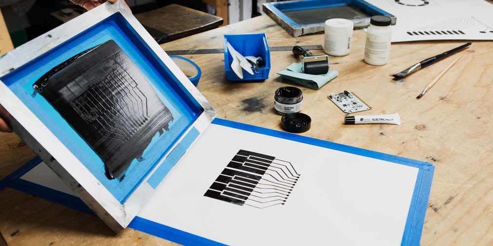
Conductive inks are advanced functional materials formulated with electrically conductive components such as silver, copper, carbon, or graphene, designed to create conductive pathways on a wide range of substrates. They are primarily used in printed electronics, enabling the production of circuits, sensors, antennas, and flexible electronic devices through cost-efficient printing techniques. The key value proposition lies in their ability to replace traditional wiring and etching processes with scalable, lightweight, and flexible solutions. Strategically, conductive inks are essential to the rapid growth of next-generation electronics, including wearable devices, IoT systems, and smart packaging, making them a critical input in modern manufacturing ecosystems.
2. Key Specifications & Technical Characteristics
- Chemical Composition:
- Silver-based (Ag), copper-based (Cu), carbon/graphite, graphene formulations
- Polymer binders, solvents, and dispersing agents
- Purity / Grade:
- High-purity metal content (typically ≥ 99.9% for metallic particles)
- Electronics-grade formulations with controlled conductivity levels
- Physical Characteristics:
- Form: հեղuids or pastes (screen, inkjet, gravure compatible)
- Color: Silver, black, or customized
- Particle size: Nano to micron-scale (10 nm – 10 µm depending on formulation)
- Viscosity: Tunable (10–50,000 cP depending on application method)
- Electrical resistivity: As low as 1–10 µΩ·cm (silver-based inks)
- Packaging Options:
- 1 kg, 5 kg, 10 kg sealed containers
- Industrial bulk drums (20–200 kg)
- Custom packaging for OEM integration
- Shelf Life:
- Typically 6–12 months under controlled storage conditions (cool, dry, sealed environment)
3. Core Industrial Applications
- Primary Industries:
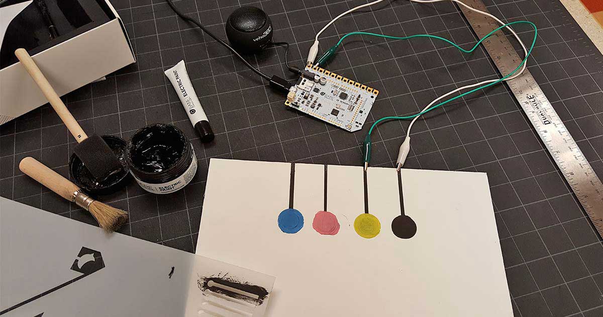
- Printed electronics and flexible electronics
- Automotive (defoggers, sensors, touch interfaces)
- Consumer electronics (RFID, NFC antennas, touchscreens)
- Renewable energy (solar cells, conductive coatings)
- Healthcare (biosensors, wearable diagnostics)
- Operational Use Cases:
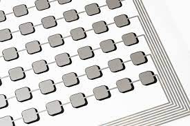
- Printing conductive traces on flexible substrates (PET, PI, paper)
- Fabrication of RFID/NFC antennas and membrane switches
- Integration into smart packaging and IoT devices
- Deposition of conductive layers in photovoltaic cells
- Performance Advantages:
- Enables low-temperature processing compared to traditional metal deposition
- Supports high-throughput roll-to-roll manufacturing
- Reduces material waste and production complexity
- Provides excellent adhesion, flexibility, and conductivity across substrates
- Efficiency & Cost Benefits:
- Lower capital expenditure vs. conventional PCB fabrication
- Faster prototyping and scalable production
- Reduced weight and material usage for end products
4. Competitive Advantages
- Quality Consistency:
- Tight control over particle size distribution and dispersion stability ensures repeatable electrical performance
- Supply Reliability:
- Scalable production capacity with consistent batch-to-batch quality assurance
- Logistics Capability:
- Global shipping with temperature-controlled handling where required
- Flexible packaging tailored to industrial procurement needs
- Price Competitiveness:
- Optimized formulations balancing performance and cost, including alternatives to high-cost silver
- Sustainability & Environmental Benefits:
- Reduced chemical waste compared to etching processes
- Lower energy consumption through additive manufacturing techniques
- Availability of eco-friendly, solvent-reduced formulations
- Technical Support:
- Comprehensive technical data sheets (TDS), safety data sheets (SDS)
- Application engineering support for process optimization and substrate compatibility
5. Commercial & Supply Information
- Minimum Order Quantity (MOQ): BULK 20MT
- Loading Capacity:
- 20–25 MT per 20-ft container (depending on packaging and formulation type)


Reviews
There are no reviews yet.